|
|
|
| General information | | For several years, the investigations dealing with the features of different silicon carbide polytypes as well as the technology of silicon carbide device manufacturing are more and more intensive. It is caused by the extremely attractive material parameters of silicon carbide in comparison to silicon ones, which is characterized by the larger band gap, the better heat conductivity, the larger electron saturation velocity and the larger critical electric field strength. These parameters, potentially, allow manufacturing silicon carbide devices characterized by ratings unattainable or attainable very difficult for the devices manufactured from silicon or other semiconductors. The large critical electric field strength allows getting high voltage p-n junctions with the breakdown voltage larger than 10 kV. The large band gap makes possible manufacturing low noise devices or devices working at high temperatures exceeding even 700°C whereas the large saturation electron velocity makes silicon carbide an excellent candidate for high frequency devices with the possible maximal frequency reaching THz. The good thermal conductivity is very crucial from the reliability point of view (thermal stresses) and thermal management problems. The basic obstacle in practical use of silicon carbide in electronics consists in different, very often extreme, demands concerning the technology processes in comparison to the processes of silicon technology. | | It causes that the technology processes and characterization procedures well know in the silicon technology occur often to be inappropriate in the case of silicon carbide. The Polish National Silicon Carbide Program is aimed at solving some of these problems and it is expected that the results of its run will create the room for further activities towards the wider introduction of silicon carbide into electronics industry. It covers several research programs gathered in three tasks, realized by 8 universities and 3 R&D units involved in SiC technology for several years. | | Scope of the Program | | The structure of the program is shown in Fig.1. It consists of three thematic tasks aimed at SiC in bulk and substrate form, SiC device manufacturing and SiC devices application, respectively. Each of the tasks covers several partially complemented projects that are carried out by separate research teams coming from different research institutions. These institutions, listed in Table 1, gather the majority of Polish research groups engaged in the investigations in silicon carbide technology and application. |
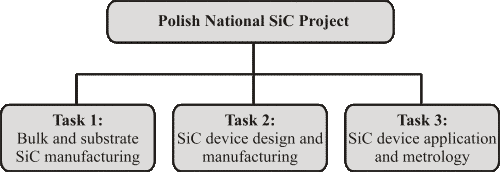
Fig. 1. Structure of the Polish National SiC Program
| | The first task is dominating in the program. Its main project is devoted to work out the technology of 6H-SiC and 4H-SiC monocrystal bulks produced from silicon carbide powder using the methods basing on Lelly approach. Other projects of this task concern next steps necessary to obtain 6H:SiC and 4H:SiC polished substrates with and without an epilayer, characterized by the quality satisfying device producers. |
Table 1. Research groups engaged in realization of Polish National SiC Program
| The second task covers projects dealing with different aspects of device manufacturing. Since the well characterized substrate is a base for any research activity aimed at semiconductor device manufacturing, a few projects is concentrated on the characterization methods specific for SiC structures, which are essential for the final results of technological processes. One of them concerns e.g. the study of electrical, optical and photoelectrical characterization methods for MIS silicon carbide structures. Other projects deal with the technology problems like the technology of selective ion implantation, which is the key process for source and drain doping in MISFET technology as well as the termination in high voltage devices, the technologies of electrical contacts for silicon carbide devices and packaging technology taking also into account the problems resulting from silicon carbide application in high temperature electronics. In this task, the separate group is formed by the projects aimed at the manufacturing technology of particular devices with the final goal to deliver the demonstrators of these devices. They deal with Schottky diodes, PiN diodes, MISFET and JFET transistors manufactured on SiC substrates as well as with high-frequency HFET transistors and Schottky diodes manufactured as AIIIN/SiC heterostructures.
The third task covers two projects only, concentrated on the investigations of advantages and disadvantages resulting from the application of SiC devices in power electronics circuits. Basing on the commercial available elements like Schottky diodes and MESFET transistors mainly, they cover the investigations of device features from the point of view of their influence on design process and work conditions in the real power electronics equipment. |
|
|